Programmable logic
Logic gates are formed by connecting transistors together on a semiconductor material to make an integrated circuit. The wafers, or chips, of semiconductor contain lots of logic gates that make up different types of devices which work together to read, store, calculate, and transmit digital information.
Most integrated circuits contain a specific arrangement logic gates at the time they are manufactured. Because of their physical and chemical properties, some semiconductors can let you change connections between the gates after the device is manufactured. By applying special voltages at programming pins, a custom arrangement of gates can be “programmed” into the integrated circuit. These types of semiconductors are part of a category of electronics called Programmable Logic Devices (PLD). There are many different kinds. Some of them you program only once and others you can erase the original gate arrangement and program in new ones multiple times.
We can use the micro:bit to create our own PLD. The digital pins are the inputs for the logic circuits. The logic gates we program are logical expressions in code that combine the digital inputs we read from the pins. The result of the expression is written to a digital output pin.
Board PLD
The physical idea of using your board as a PLD looks like this:
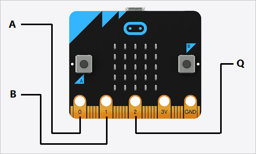
The logic inputs for A and B are connected to digital input pins. The resulting output Q is connected to a digital output pin. We can make a general representation of your board as a PLD by selecting some digital pins to use as inputs and outputs for our programmable logic.
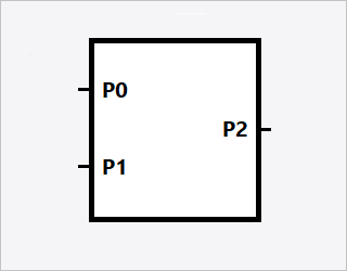
By “connecting” the pins together with code, we can program virtual logic gates and make the board act like a PLD. With multiple pins and some more code, we can even create a combined logic circuit.

Programmable NOT gate
The NOT gate takes the logic value of the input and inverts it at the output. This is a single input gate using just the P0 pin for input.

The NOT gate is wired using alligator test clips as shown in the following diagram. The output clip is connected to pin P2.
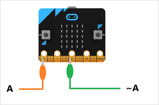
The script to program the NOT gate is simply a logical inverse of ||pins:digital read pin|| written to an output pin with ||pins:digital write pin||.
if (pins.digitalReadPin(DigitalPin.P0) > 0) {
    pins.digitalWritePin(DigitalPin.P2, 0)
} else {
    pins.digitalWritePin(DigitalPin.P2, 1)
}
Programmable OR gate
The OR gate takes two inputs and makes the output true if any input is true. The P0 and P1 pins are the inputs.
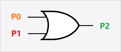
The OR gate is wired using alligator test clips as shown in this diagram. The output clip is connected to pin P2.
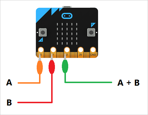
The script to program an OR gate is two ||pins:digital read pin|| blocks, evaluated with an ||logic:or||, and the result is written to an output pin with ||pins:digital write pin||.
if ((pins.digitalReadPin(DigitalPin.P0) > 0) || pins.digitalReadPin(DigitalPin.P1) > 0) {
    pins.digitalWritePin(DigitalPin.P2, 1)
} else {
    pins.digitalWritePin(DigitalPin.P2, 0)
}
Programmable AND gate
The AND gate takes two inputs and makes the output true if both inputs are true. The P0 and P1 pins are the inputs.
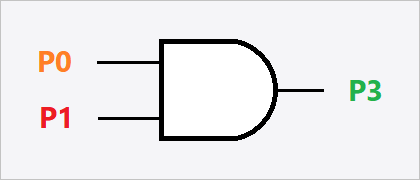
The AND gate is wired using alligator test clips as shown in the next diagram. The output pin is connected to pin A2.

The script for an AND gate is two ||pins:digital read pin|| blocks, evaluated with an ||logic:and||, and the result is written to an output pin with ||pins:digital write pin||.
if ((pins.digitalReadPin(DigitalPin.P0) > 0) && pins.digitalReadPin(DigitalPin.P1) > 0) {
    pins.digitalWritePin(DigitalPin.P2, 1)
} else {
    pins.digitalWritePin(DigitalPin.P2, 0)
}
Combined logic
You can program your board to have multiple logic gates that operate on the two inputs. Just combine the three logic gate scripts from above into one ||loops:forever|| loop. If you have an expansion connector for your micro:bit, you could program multiple outputs for your logic system. You could also use one extra input pin as an observer pin to test the outputs of your combined logic. The different outputs feedback to the observer pin so it will see what their logic levels are. Here’s a schematic for a multiple gate system.
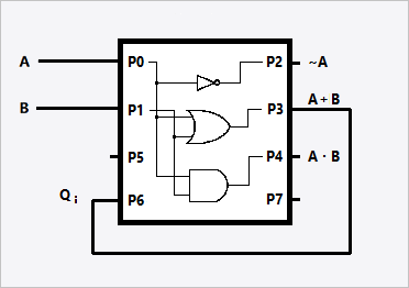
The combined logic for our multiple gate PLD is programmed like this:
let A = false
let B = false
basic.forever(function () {
    A = pins.digitalReadPin(DigitalPin.P0) > 0
    B = pins.digitalReadPin(DigitalPin.P1) > 0

    if (A) {
        pins.digitalWritePin(DigitalPin.P2, 0)
    } else {
        pins.digitalWritePin(DigitalPin.P2, 1)
    }
    if (A || B) {
        pins.digitalWritePin(DigitalPin.P3, 1)
    } else {
        pins.digitalWritePin(DigitalPin.P3, 0)
    }
    if (A && B) {
        pins.digitalWritePin(DigitalPin.P4, 1)
    } else {
        pins.digitalWritePin(DigitalPin.P4, 0)
    }
    basic.pause(100)
})
Logic observer
As easy way to see what the outputs of our PLD are, you can use the P6 pin as a logic observer input and display the letter T for a true output value and the letter F for false.
basic.forever(function () {
if (pins.digitalReadPin(DigitalPin.P6) > 0) {
        basic.showString("T")
    } else {
        basic.showString("F")
    }
    basic.pause(100)
})
Input tests
You can test different input combinations by connecting the other ends of alligator clip leads on pins P0 and P1 to either GND or 3V. The GND pin will make a false input value and 3V will make a true input value.
If you have an expansion connector for your micro:bit, you can use the combined logic script and the logic observer code to check each ouptput. Move the other end alligator clip lead connected to the observer pin P6 to each of the outputs P2, P3, and P4 to see the result of the logic operation programmed for those pins.
If you just have the micro:bit by itself, you can test each logic function using only the scripts for each logic gate. Just put the script inside a ||loops:forever|| and place a ||basic:show string|| block with the logic letter after each ||pins:digital write pin||.
This is the code for the NOT gate:
basic.forever(function() {
    if (pins.digitalReadPin(DigitalPin.P0) > 0) {
        pins.digitalWritePin(DigitalPin.P2, 0)
        basic.showString("F")
    } else {
        pins.digitalWritePin(DigitalPin.P2, 1)
        basic.showString("T")
    }
    basic.pause(100)
})
NOT truth table
As an example, here’s the truth table with pin voltages for the NOT operation:
| P0 | P2 | Display |
|---|---|---|
| GND | 3V | [basic.showString("T")] |
| 3V | GND | [basic.showString("F")] |
Do test connections for the inputs and check the results for the OR and AND outputs.
OR truth table
| P0 | P1 | P3 | Display |
|---|---|---|---|
| GND | GND | ? | ? |
| GND | 3V | ? | ? |
| 3V | GND | ? | ? |
| 3V | 3V | ? | ? |
AND truth table
| P0 | P1 | P4 | Display |
|---|---|---|---|
| GND | GND | ? | ? |
| GND | 3V | ? | ? |
| 3V | GND | ? | ? |
| 3V | 3V | ? | ? |
XOR device
As we learned earlier, the XOR gate operation is made up from several other gates. The result Q was made from this expression in code:
let A = false
let B = false
let Q = (!A && B) || (A && !B)
We’ll make an XOR gate by programming a combined logic device for it. This time let’s say that the whole micro:bit is a programmed XOR gate.
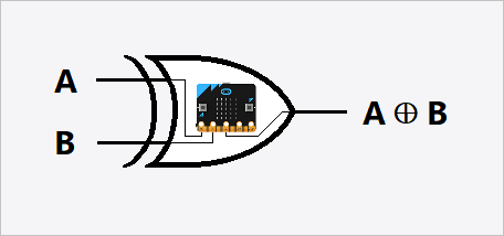
Let’s use the same wiring diagram as we did for the OR gate using P0 and P1 as input pins with P2 as the output pin.
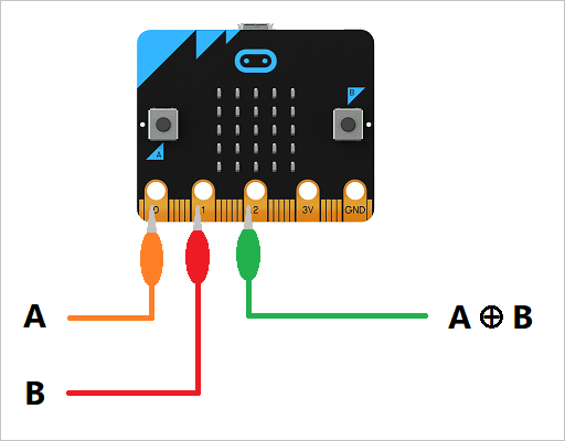
Our logic gate script is a bit different this time. To simplify forming the expression for XOR, we’ll assign variables to the input and output values.
let A = false
let B = false
basic.forever(function () {
    A = pins.digitalReadPin(DigitalPin.P0) > 0
    B = pins.digitalReadPin(DigitalPin.P1) > 0
    if (!(A) && B || A && !(B)) {
        pins.digitalWritePin(DigitalPin.P2, 1)
        basic.showString("T")
    } else {
        pins.digitalWritePin(DigitalPin.P2, 0)
        basic.showString("F")
    }
    basic.pause(100)
})
Connect the inputs for P0 and P1 according to the XOR truth table and see if the outputs in the table match your results.
| P0 | P1 | P2 | Display |
|---|---|---|---|
| GND | GND | GND | [basic.showString("F")] |
| GND | 3V | 3V | [basic.showString("T")] |
| 3V | GND | 3V | [basic.showString("T")] |
| 3V | 3V | GND | [basic.showString("F")] |